


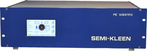
 plasma cleaning machine / for the electronics industry / with filtration system
SEMI-KLEEN quartz
INO Group
Request for quotation
Products relative
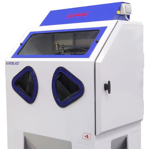
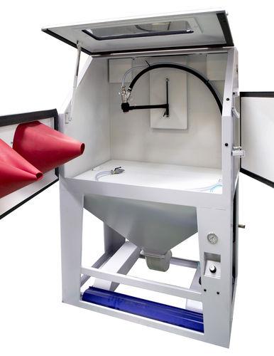
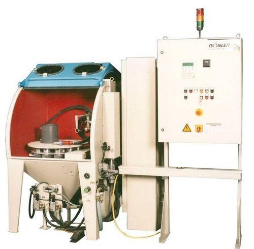
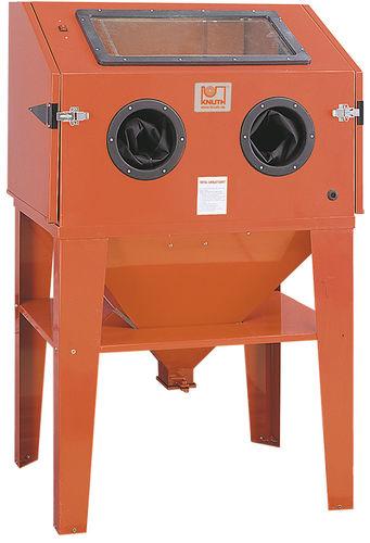
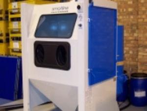
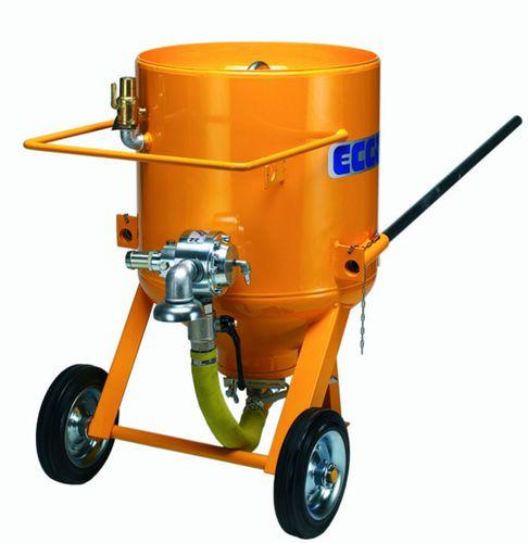
Sand-blasting machines, sand-blasting cabinets, sand-blasting guns
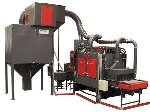
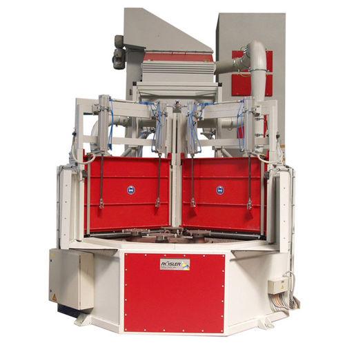
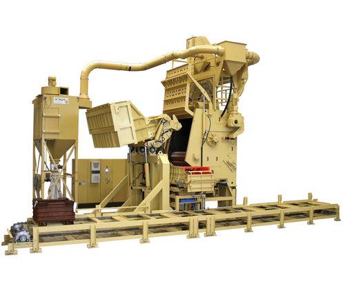
Shot-blasting machines, shot-peening machines, shot-blasting booths
CNC polishing machines, belt sanders, bench grinders